
(Untitled)
I was pretty sure this was going to be another doomed sample.
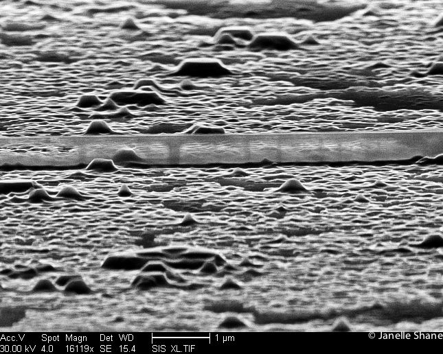
For one, none of those little mesas and bumps - all formed of semiconductor laser material - were supposed to be there. It was all very interesting-looking, but it meant that some kind of junk had gotten on my sample and left its imprint while I was trying to form the laser-material wall.
And the laser-material wall was definitely not supposed to be transparent. I didn’t even know they could be transparent. I took these pictures with a scanning electron microscope, and the fact that we can look right through the side of these walls means that that the electron beam is going clear through the side of these walls twice, once on the way through and once on the way back. I’m not sure how thin the walls have to be to allow it to do that, but I’m guessing not many atoms thick.
If I were trying to make them that thin, I’d be pretty proud of myself.
Fortunately, I ended up managing to save this sample. I chucked it in a plasma cleaner that got rid of whatever junk was covering the little mesas and plateaus. Then when I etched it again, all the little bumps disappeared. I sent the chip to the dicer to chop off the ridiculously thin parts. It looks less interesting now (except for a new visitor I dubbed “Dustzilla”), but it should be usable. On to science!
