Sunday February 02, 2014

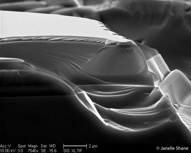
Fracture patterns at the edge of a broken wafer (broken on purpose, for once). The lighter top layer is silicon, and the darker bottom layer is glass. The glass looks darker than the silicon because it’s a better electrical insulator - the electron beam microscope makes an image by scanning a beam of electrons across a sample and looking at how many electrons get bounced up to a detector. If an area reflects very few electrons, it appears dark. Since glass is an electrical insulator, it tends to absorb most of the electrons rather than reflecting them, so the glass in this image looks dark. Silicon’s less electron-hungry, so it appears brighter. Since the detector’s located above the sample in this view, you also get light and shadow - light where surfaces face the detector, and shadows beneath overhangs.


