AI Weirdness: the strange side of machine learning

Tag: nanolandscape

Total 30 Posts
(Untitled)

(Untitled)

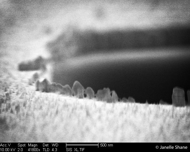
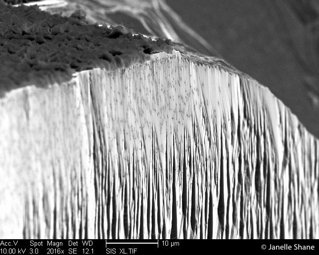
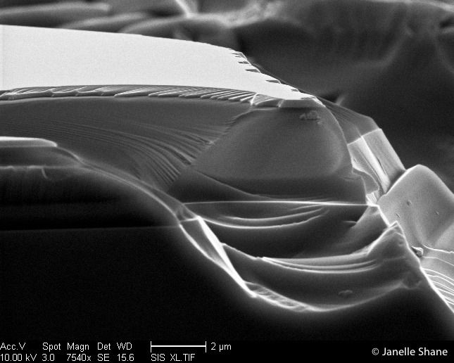
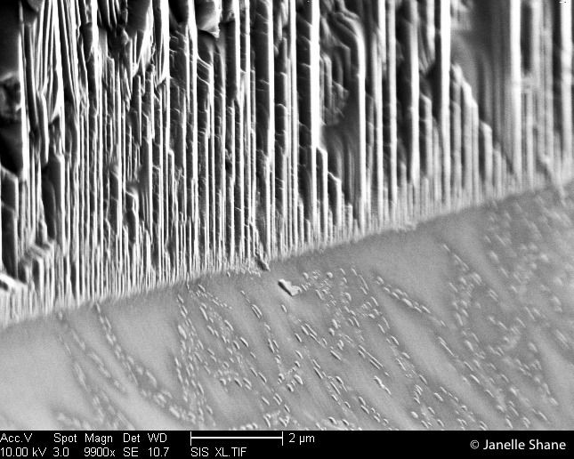
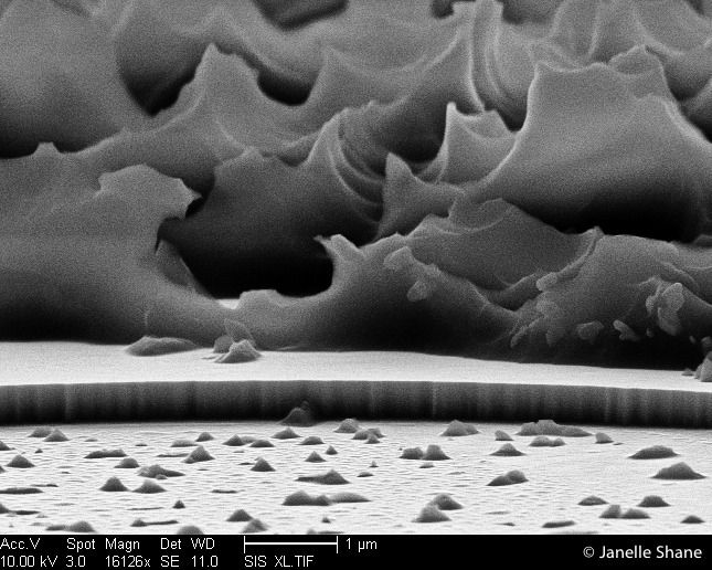
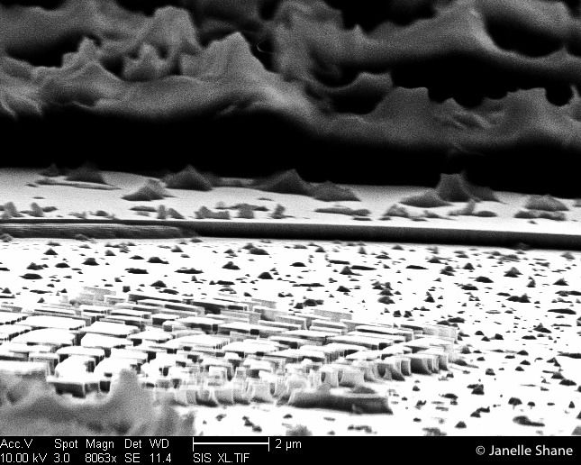
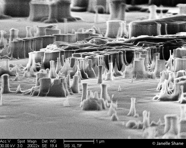
The beachgoers flee as hulking monsters climb from the dark water… 
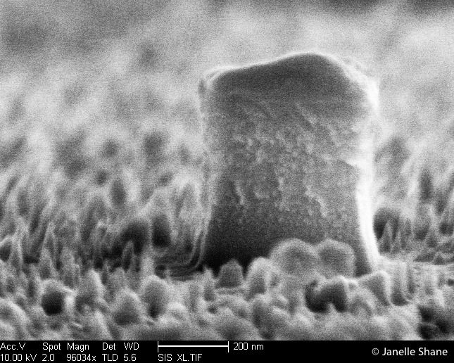
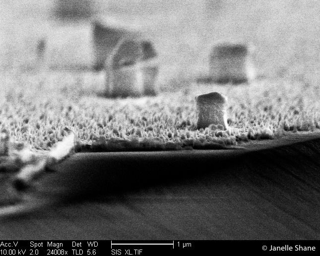
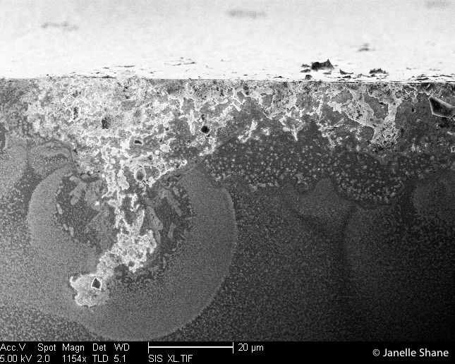
This is a scanning electron microscope image of some various-sized pillars that appeared on one of my samples during a plasma etching test.  They’re made of semiconductor, and the bright plain beneath is silicon.  Showing through the dark
(Untitled)

(Untitled)

The microscopic fractured edge of a piece of semiconductor looms like an enormous cliff face.  However, this entire view would fit easily inside the diameter of a single human hair.  At the top of the cliff is a rough dark layer, the remains of a protective layer that we bombarded
(Untitled)

(Untitled)

Fracture patterns at the edge of a broken wafer (broken on purpose, for once).  The lighter top layer is silicon, and the darker bottom layer is glass.  The glass looks darker than the silicon because it’s a better electrical insulator - the electron beam microscope makes an image by
(Untitled)

(Untitled)

Microscopic fracture patterns appear clifflike on the edge of one of my samples.  This entire view is less than 10 micrometers high, meaning that it covers about a tenth the thickness of a typical human hair.  We usually don’t get patterns like these, because we use a special wafer
(Untitled)

(Untitled)

The crazy-huge mountains of the nanoworld!  The strange waves and scallops are what is left of the protective mask I used to shield the semiconductor material below from a high-energy etching plasma.  The mask held up to the plasma, although it was probably damaged a bit - and then I
(Untitled)

(Untitled)

A mini-monument, made of semiconductor laser material.  It looks to me a bit like Devil’s Tower.  It’s much, much smaller, though.  Scaling this little nano-tower (600nm high) to the height of Devil’s Tower (386m high) would be like scaling up an average-sized human (~1.7m) to about
(Untitled)

(Untitled)

Coastline of the land of monuments… tiny monuments.  Each of them would fit easily inside a single human cell.  They’re formed out of semiconductor, and are the result of what we call micromasking: tiny bits of debris landed on the semiconductor before the etching step, and protected the semiconductor
(Untitled)

(Untitled)

Frostlike patterns emerge when acetone partially dissolves a plasticy layer of old photoresist.  This is the same sample as in my previous post [http://tmblr.co/ZP7VLs_nDmsM], which used to be covered in jagged black mountains made of plasma-damaged photoresist. Now the mountains are mostly dissolved away, except for
(Untitled)

(Untitled)

This image is from a test of our plasma etcher, and shows a white plain of semiconductor laser material etched partially away by plasma.  In the background is the black remains of photoresist that was protecting other areas of semiconductor from being etched - it did the job, but took
(Untitled)

(Untitled)

A strange miniature landscape, none of which is supposed to be there.  It’s quite small indeed - the pinnacles are each less than 1 micrometer tall, which means you’d need to stack a thousand of them on top of each other to equal one millimeter. This landscape is
You've successfully subscribed to AI Weirdness
Great! Next, complete checkout for full access to AI Weirdness
Welcome back! You've successfully signed in.
Unable to sign you in. Please try again.
Success! Your account is fully activated, you now have access to all content.
Error! Stripe checkout failed.
Success! Your billing info is updated.
Error! Billing info update failed.