
Thursday May 08, 2014
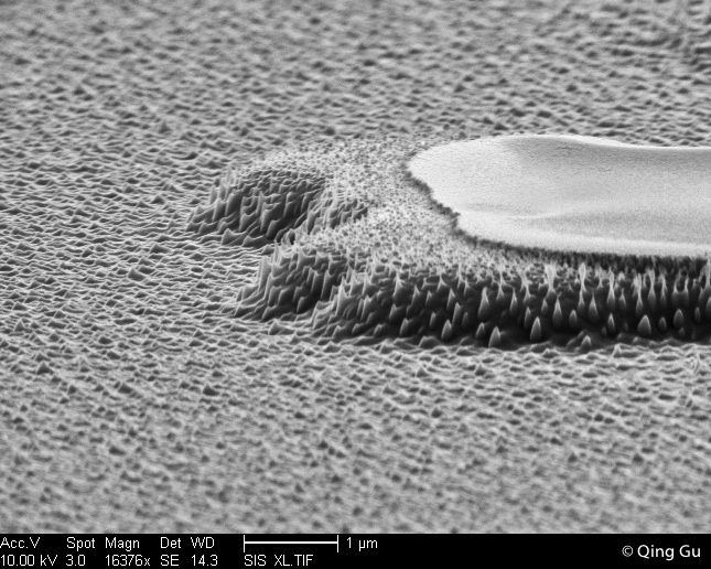
Strange formations caused when high-energy plasma from a reactive ion etcher bombards semiconductor materials.
We use the reactive ion etcher to carve out microscopic optical devices, like lasers and filters. Here, there’s no particular device that we were trying to make - we were just testing to see if the etching worked, so we resorted to the very quick-and-easy method of just sticking a bit of tape over part of the sample. Sure enough, there was a difference between the tape-shielded area over to the right and the non-shielded area. The transitions between the two regions aren’t very sharp, but we’re not really expecting a lot out of a piece of tape. The tape’s already been removed for this picture - otherwise, it would loom about 100x higher than everything else in the picture.
Tape-applying, etching, and electron microscope imaging - everything, in other words - was done by my labmate Dr. Qing Gu. (Dr. as of a week ago, so she probably still thinks her name looks weird written this way)
