

Wednesday July 03, 2013
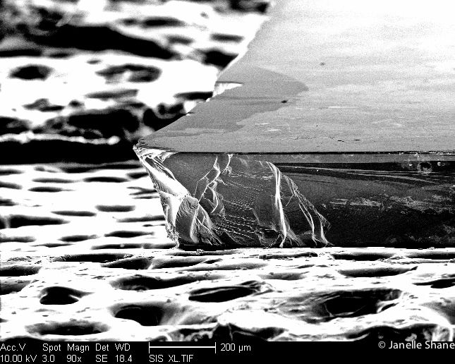
Someone asked me yesterday how big my samples are, and what it all looks like. This is a zoomed-out view (only 90x!) showing a nearly edge-on view of one of my samples, sitting on a cratered sea of carbon tape. It’s so zoomed-out that I almost feel embarrassed asking the electron microscope to image this… my typical magnifications are more like 100,000x.
Typically, my samples are about 300 microns thick, which is about the thickness of three hairs stacked on top of each other, or slightly thinner than an extra-light guitar pick. In size they vary a lot - this one is about 0.5cm x 1cm. I’ve worked with smaller ones, but then they get difficult to handle with tweezers, and the risk of disaster greatly increases.
Most of what you see here in the cross section is silicon. There’s a thin layer of glass on the top (visible as a dark stripe), and above that is an even thinner layer of semiconductor laser material. This sample is still nice and thick - I have a coworker who uses much thinner samples, so thin that the edges flake and crumble when she picks them up with tweezers.
