

Wednesday September 18, 2013
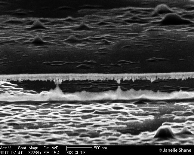
Nanoscale forces work in non-intuitive ways sometimes. This wall of semiconductor was plasma-etched so thin that the middle was etched entirely away, leaving the wall’s top floating eerily above void. It’s thin and lacy, and only touches the wall’s bottom in a few delicate places, yet it doesn’t fall, even when I shuttle the sample from building and move it in and out of the electron microscope. It’s terrifically small - a single virus could slip through the gap, but a bacterium couldn’t, and a human cell certainly couldn’t.
The surrounding area is rough and mountainous because of some kind of crud that was on the sample surface during the first plasma etching. A round of microwave plasma treatment, followed by a bit more plasma etching, smoothed everything down.
