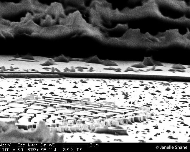
This image is from a test of our plasma etcher, and shows a white plain of
semiconductor laser material etched partially away by plasma. In the background
is the black remains of photoresist that was protecting other areas of
semiconductor from being etched - it did the job, but took some