
(Untitled)

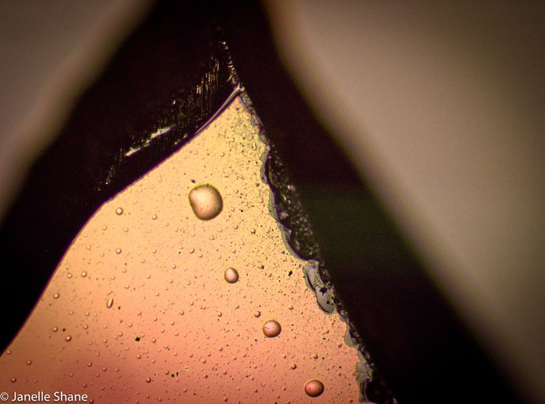
Here’s the jagged edge where my sample broke.
I blame the carbon tape, which is usually my friend, a nice way to get rid of those pesky extra electrons, and a way to stop my sample from falling off the holder in the electron microscope. Except this time, the tape did its job too well, and wouldn’t relinquish its hold on my sample. As I tried to pry it up with tweezers, it cracked and splintered. Luckily, the largest piece still had my pattern on it, and I managed to pry it loose with a razor blade before I damaged it further.
Thanks to the break, you can see all three materials this sample is made out of. The top layer - which is rainbow-colored due to its thinness - is semiconductor laser material. Beneath that in grey is silicon dioxide - good old glass. Finally at the bottom is a thick chunk of nearly-black silicon. I have no idea why it’s doing its impression of a frosty can of pop… those aren’t beads of condensation. I may find out when I go to look at this sample again with the electron microscope.
