
(Untitled)

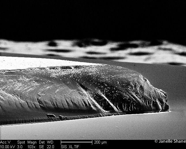
I posted a picture of the jagged broken edge of my sample the other day. Now here’s the same spot under the electron microscope. This view’s looking from the side, so you see all the detail of the dark edge where the silicon snapped.
This far zoomed out, the landscape’s made out of a bunch of different materials. There’s a really thin layer of glass above the dark silicon, too thin to make out in this view, and above that is a layer of even thinner semiconductor laser material. Below the broken silicon is a smooth surface of polished silicon (I’m using it as a platform to carry the smaller silicon/laser piece around on). The cratered surface at the back of the picture is carbon tape.
Subscribe now
Already have an account? Sign in
