(Untitled)
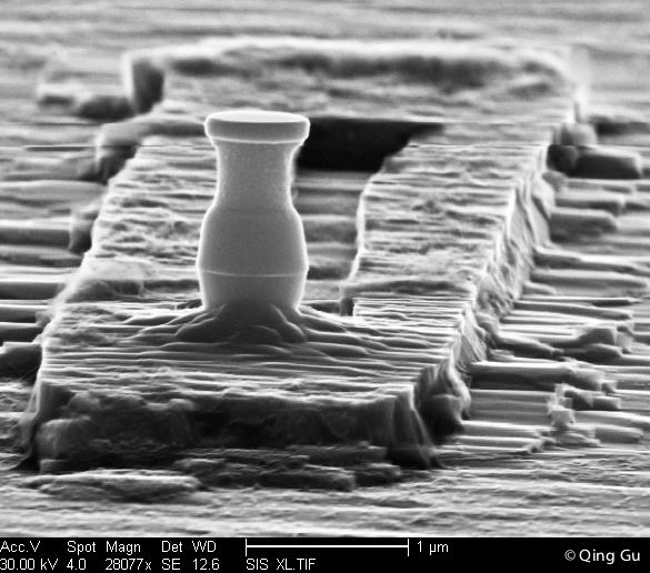
When a nanolaser casts a shadow, the grad student gets 6 more weeks of fabrication.
The pillar in the middle is one of the nanolasers our lab makes. It’s supposed to be a single column all by itself, roughly cylindrical with a bit of a funky coke bottle shape, about 1/100 the height of a sheet of printer paper. We etch out the column from a solid block of layered semiconductor, using a bombardment of high-energy plasma from the top. So, how did the nanolaser end up carving its shadow into solid semiconductor?
It seems that when we use the scanning electron microscope (SEM) to look at our nanolasers after various steps in our fabrication process, the microscope’s electron beam changes the properties of the semiconductor it hits, making it more resistant to our etching plasma. Since we’re usually imaging our lasers from the side, the electron beam hits each nanolaser pillar at an angle, and the area hidden behind the nanolaser gets shielded from the beam.
What this means, unfortunately, is that the more we use SEM to look at our fabrication progress, the less predictable the fabrication process becomes. A watched laser never lases.
Fabrication and SEM by Dr. Qing Gu.
