AI Weirdness: the strange side of machine learning

Tag: scanning electron microscope

Total 75 Posts
(Untitled)

(Untitled)

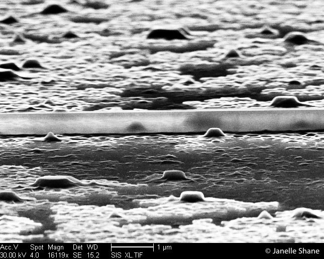
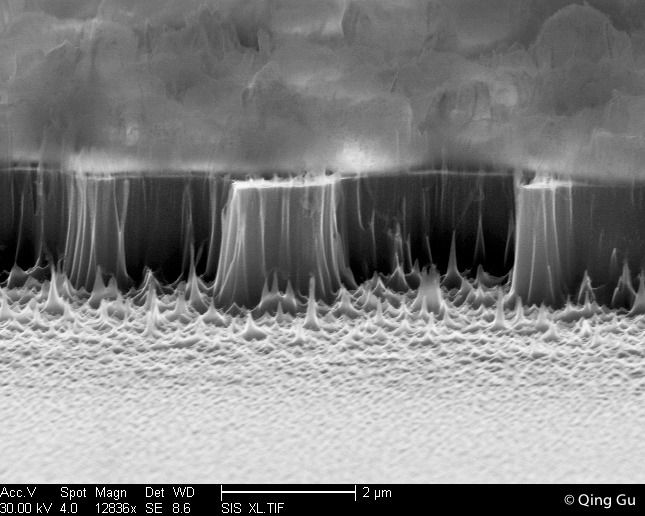
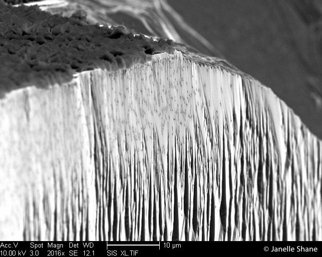
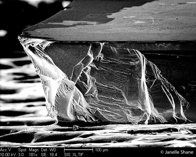
It looks like it could be an image of desert badlands - except for that strangely translucent wall.  In fact, this scene is much, much smaller. An ant could step over the wall without ever noticing its existence. This image was taken through an electron microscope, of a microscopic landscape
(Untitled)

(Untitled)

Resembling arrays of flaming islands, these formations are actually microscopic, etched out of semiconductor. This semiconductor material is what we use to make microscopic lasers - we start with a vast, featureless sheet of semiconductor and cover certain areas with a protective layer of glassy photoresist.  Then we blast the
(Untitled)

(Untitled)

It resembles a mushroom cloud, but in fact, it’s one of our microscopic nanolasers, imaged under an electron microscope.  These lasers are among the smallest in the world, so small you could fit a billion of them on an iPhone home button, small enough to one day fit easily
(Untitled)

(Untitled)

Strange formations caused when high-energy plasma from a reactive ion etcher bombards semiconductor materials. We use the reactive ion etcher to carve out microscopic optical devices, like lasers and filters.  Here, there’s no particular device that we were trying to make - we were just testing to see if
(Untitled)

(Untitled)

The cliffs of fluffiness!  Lashed by impossibly pointy nano-waves. The fluffy stuff at the top is actually photoresist, a glassy substance that we use to protect semiconductor from plasma bombardment when we’re doing our etching.  Here, the photoresist protected the semiconductor below it from being etched away, making the
(Untitled)

(Untitled)

Sometimes the view under an electron microscope can be positively scary.  I’ll be scrolling along at low magnification, checking out some nanoscale features, when all of a sudden a colossus will loom huge above the nanolandscape.  Sometimes I actually jump.  Usually it’s a tiny microscopic speck of dust,
(Untitled)

(Untitled)

The long valley, surrounded by jagged mountains, occupied by a picturesque leaning castle….  Actually, this is a closeup of a minuscule scratch in a coating of photoresist.  At this magnification (2096x), it’s clear that the photoresist has a rough, mountainous surface, caused by the high-energy plasma I’d bombarded
(Untitled)

(Untitled)

The beachgoers flee as hulking monsters climb from the dark water… This is a scanning electron microscope image of some various-sized pillars that appeared on one of my samples during a plasma etching test.  They’re made of semiconductor, and the bright plain beneath is silicon.  Showing through the dark
(Untitled)

(Untitled)

The microscopic fractured edge of a piece of semiconductor looms like an enormous cliff face.  However, this entire view would fit easily inside the diameter of a single human hair.  At the top of the cliff is a rough dark layer, the remains of a protective layer that we bombarded
(Untitled)

(Untitled)

A rare view of the entire cross-section of one of my samples, which seems to loom like a massive iceberg over choppy seas. This sample is a thin layer of semiconductor (a material we use for making lasers, among other things), bonded to a much thicker chunk of glass.  The
You've successfully subscribed to AI Weirdness
Great! Next, complete checkout for full access to AI Weirdness
Welcome back! You've successfully signed in.
Unable to sign you in. Please try again.
Success! Your account is fully activated, you now have access to all content.
Error! Stripe checkout failed.
Success! Your billing info is updated.
Error! Billing info update failed.